main
go back
16b2x CPU
date: 2022-05 ; 2023-01 ; 2023-04
desc: second CPU design, mostly fixes from previous designs ; implemented unified memory ; first CPU written in VHDL
proj: https://github.com/sarvl/16b2x
Table Of Contents
- Overview
- ISA
- Unified Memory
- VHDL
- The Good
- The Bad
- The Ugly
OVERVIEW

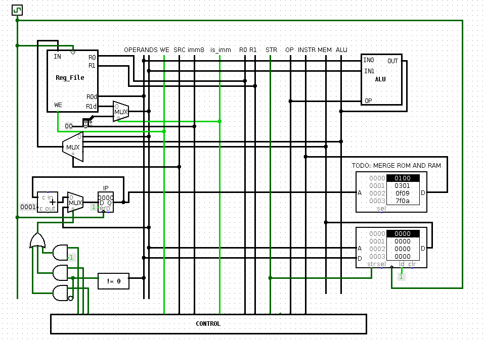
full image
As with previous design, this CPU was initially done in logisim.
This time there were no major flaws in the ISA, general layout was somewhat inspired by SAP from Digital Computer Electronics (same thing that Ben Eater used for 8 bit computer).
Pretty much everything that had to be fixed from previous design, was fixed
As the note near ROM/RAM (and as some features of ISA, described below) suggests, project was not fully complete then .

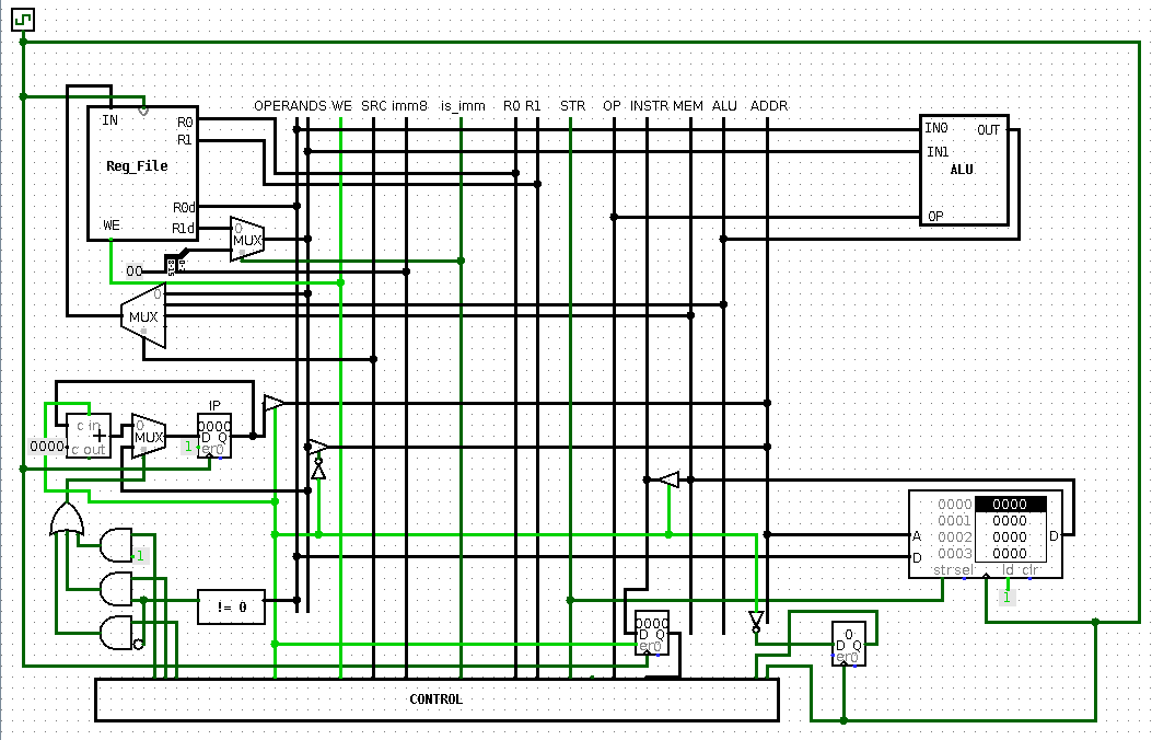
full image
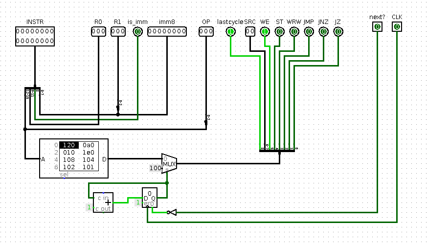
New circuitry allowed instructions to execute for 2 cycles which is essential for unified data and instruction memory.
Most instructions execute in 1 cycle as in previous iteration, but loads and stores take 2 cycles.
During 1st they access data, during 2nd they access next instruction

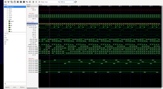
full image
First major-ish project in VHDL so code is not as good as it should be, entire project is in single file, including tests.
The implementation does not have multicycle instructions for simplicity, same as first iteration of the entire project.
ISA
Instructions:
- mov Rd, Rs/imm8 # Rd <-- Rs/imm8
- ldw Rd, Rs/imm8 # Rd <-- M[Rs/imm8]
- stw Rd, Rs/imm8 # M[Rs/imm8] <-- Rd
- rdw Rd, Rs/imm8 # Rd <-- P[Rs/imm8]
- wrw Rd, Rs/imm8 # P[Rs/imm8] <-- Rd
- jmp Rs/imm8 # IP <-- Rs/imm8
- jnz Rd, Rs/imm8 # if(Rd != 0) IP <-- Rs/imm8
- jz Rd, Rs/imm8 # if(Rd == 0) IP <-- Rs/imm8
- add Rd, Rs/imm8 # Rd <-- Rd + Rs/imm8
- sub Rd, Rs/imm8 # Rd <-- Rd + Rs/imm8
- not Rd, Rs/imm8 # Rd <-- ~ Rs/imm8
- and Rd, Rs/imm8 # Rd <-- Rd & Rs/imm8
- or Rd, Rs/imm8 # Rd <-- Rd | Rs/imm8
- xor Rd, Rs/imm8 # Rd <-- Rd ^ Rs/imm8
- sll Rd, Rs/imm4 # Rd <-- Rd << Rs/imm4
- slr Rd, Rs/imm4 # Rd <-- Rd >> Rs/imm4
M[x] refers to accessing memory at address x
P[x] refers to accessing IO port with id x (not implemented in any iteration)
Instruction Format:
	AAAABBBC XXXXXXXX

	AAAA - opcode
	BBB  - Rd id
	C    - if 1 then second operand is immediate, otherwise it is register
	X3   - Rs
	X4   - imm4
	X8   - imm8

	Xn means rightmost n bits of X
Example Program:
	mov 	R0, 0
	mov 	R1, 1

	#computes nth fib number
	mov 	R7, 9

	jz  	R7, end
loop:
	stw 	R0, 0

	mov 	R2, R0
	mov 	R0, R1
	add 	R1, R2

	sub 	R7, 1
	jnz 	R7, loop

end:
	mov 	R0, R0 #nop for assembler to place label correctly
UNIFIED MEMORY
The main goal of this project was to unify memory
Unfortunately I do not remember attemps too well but the entire approach was very convoluted and ultimately could not work.
Idea was to check whether data is already out and if so switch address (during the same cycle).
This cannot work because there is nothing that stores the first result so a register has to be added.
But a register cannot just store data whenever and has to wait for clock so the only solution is to have multicycle operation.
Note 1: There is another slight problem with checking availability of data - logisim RAM outputs data almost immediattely and does not signal whether it is ready.
Note 2: Even with latch (which does not update on edge) something like clock has to be used to decide when to update that latch.
Note 3: Updating on half cycle works too but that behaves identically (from digital logic POV) as twice as fast clock.
After taking long break and accepting multicycle operation, unified memory worked pretty much instantly.
CPU was not designed with more than 1 CPI in mind and it was kind of hacked in.
Each instruction has last cycle in control signals and if it is set then instruction is fetched to Instruction Register, this is usually the case.
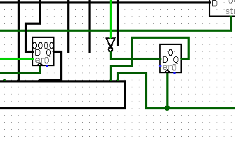
If it is NOT set then IR is not updated and '1' is written to additional 1b register acting as current-cycle register.
This external register is rather annoying to work with, next designs fixed this problem by properly incorporating notion of execution cycle.
Use of Async reset here was some wild thinking done my part.

full image

full image
VHDL
VHDL here was mostly like processor design of the 16b1x - giant pile of mess, not knowing what I am doing and trying to make things work.
921 lines of entities with their testbenches and CPU.
Most of which is VHDL boilerplate and actual logic is simple, CPU body (connections between components and logic) has only 60 LOC, most of which are whitespace or VHDL keywords.
Other than that, it is almost 1:1 translation of first iteration.
THE GOOD
No disasters and fixed previous mistakes!
Instructions were allocated properly and format is pleasant to write assembler for.
Overall layout is also much nicer to look at however individual components are mostly identical as in 16b1x.
THE BAD
No stupidly bad decisions and mistakes like last time, all are minor enough to land in THE UGLY.
THE UGLY
Did not use ports even though they are somewhat specified in the ISA
NOP slide is still present and there is no halt instruction so CPU always executes
main
go back
